Ordering number : ENN7065A
D0102AS (OT) No. 7065-1/5
Overview
The STK402-000 series products are audio power
amplifier hybrid ICs that consist of optimally-designed
discrete component power amplifier circuits that have
been miniaturized using SANYO's unique insulated metal
substrate technology (IMST). SANYO has adopted a new
low thermal resistance substrate in these products to
reduce the package size by about 60% as compared to the
earlier SANYO STK407-000 series.
Features
∑ Series of pin compatible power amplifiers ranging from
20 W
◊
2 channels to 120 W
◊
2 channels (10%/1 kHz)
devices. The same printed circuit board can be used
depending on the output power grade.
∑ The pin arrangement is compatible with that of the 3-
channel STK402-200 series. This means that 3-channel
printed circuit boards can also be used for 2-channel
products.
∑ Miniature packages
-- 15 W/ch to 40 W/ch (THD = 0.4%, f = 20 Hz to
20 kHz); 46.6 mm
◊
25.5 mm
◊
8.5 mm *
-- 50 W/ch to 80 W/ch (THD = 0.4%, f = 20 Hz to
20 kHz); 59.2 mm
◊
31.0 mm
◊
8.5 mm *
*: Not including the pins.
∑ Output load impedance: R
L
= 6
∑ Allowable load shorted time: 0.3 seconds
∑ Supports the use of standby, muting, and load shorting
protection circuits.
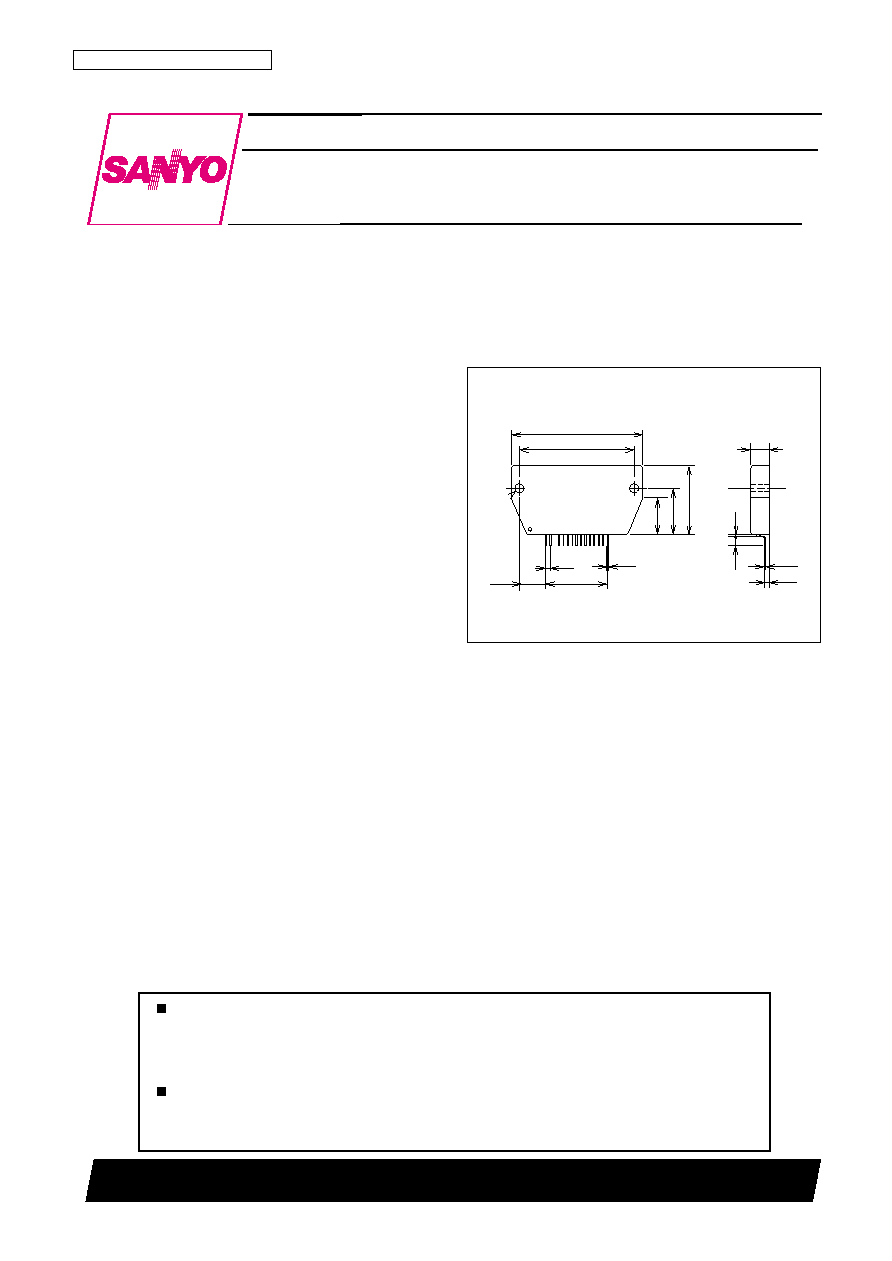
Package Dimensions
unit: mm
4190-SIP15
59.2
52.0
(12)
¯3.6
2.0
14X2=28
0.5
15
8.5
0.4
2.9
16.5
21.0
4.0
1.0
31.0
1
SANYO: SIP15
[STK402-090]
STK402-090
SANYO Electric Co.,Ltd. Semiconductor Company
TOKYO OFFICE Tokyo Bldg., 1-10, 1 Chome, Ueno, Taito-ku, TOKYO, 110-8534 JAPAN
Two-Channel Class AB Audio Power Amplifier IC
50 W + 50 W
Thick-Film Hybrid IC
Any and all SANYO products described or contained herein do not have specifications that can handle
applications that require extremely high levels of reliability, such as life-support systems, aircraft's
control systems, or other applications whose failure can be reasonably expected to result in serious
physical and/or material damage. Consult with your SANYO representative nearest you before using
any SANYO products described or contained herein in such applications.
SANYO assumes no responsibility for equipment failures that result from using products at values that
exceed, even momentarily, rated values (such as maximum ratings, operating condition ranges, or other
parameters) listed in products specifications of any and all SANYO products described or contained
herein.
No. 7065-2/5
STK402-090
Item
Type No.
STK402-020
STK402-030
STK402-040
STK402-050
STK402-070
STK402-090
STK402-100
STK402-120
Output 1 (10%/1 kHz)
20 W + 20 W
30 W + 30 W 40 W + 40 W
45 W +45 W
60 W + 60 W
80 W + 80 W 100 W + 100 W 120 W + 120 W
Output 2 (0.4%/20 Hz to 20 kHz) 15 W + 15 W
20 W + 20 W 25 W + 25 W
30 W + 30 W
40 W + 40 W
50 W + 50 W
60 W + 60 W
80 W + 80 W
Maximum supply voltage
±30 V
±34 V
±38 V
±40 V
±50 V
±54 V
±57 V
±65 V
(No signal)
Maximum supply voltage
±28 V
±32 V
±36 V
±38 V
±44 V
±47 V
±50 V
±57 V
(6
)
Recommended supply voltage
±19 V
±22 V
±25 V
±26.5 V
±30 V
±32 V
±35 V
±39 V
(6
)
Package
46.6 mm
◊
25.5 mm
◊
8.5 mm
59.2 mm
◊
31.0 mm
◊
8.5 mm
Series Organization
Parameter
Symbol
Conditions
Ratings
Unit
Maximum supply voltage (No signal)
V
CC
max(0)
±54
V
Maximum supply voltage
V
CC
max(1) R
L
= 6
±47
V
Thermal resistance
j-c
Per power transistor
2.2
∞C/W
Junction temperature
Tj max
Both the Tj max and the Tc max conditions must be met.
150
∞C
Operating IC substrate temperature
Tc max
125
∞C
Storage temperature
Tstg
≠30 to +125
∞C
Allowable load shorted time
*
2
ts
V
CC
= ±32.0 V, R
L
= 6
, f = 50 Hz, P
O
= 50 W
0.3
s
Specifications
Maximum Ratings
at Ta = 25∞C
These products are organized as a series based on their output capacity.
Parameter
Symbol
Conditions
*
1
Ratings
Unit
V
CC
(V)
f (Hz)
P
O
(W)
THD (%)
min
typ
max
Output power
P
O
(1)
±32.0
20 to 20 k
0.4
47
50
W
P
O
(2)
±32.0
1 k
10
80
Total harmonic distortion
THD (1)
±32.0
20 to 20 k
1.0
VG = 30 dB
0.4
%
THD (2)
±32.0
1 k
5.0
VG = 30 dB
0.01
Frequency characteristics
f
L
, f
H
±32.0
1.0
+0 ≠3 dB
20 to 50 k
Hz
Input impedance
ri
±32.0
1 k
1.0
55
k
Output noise voltage
*
3
V
NO
±39.0
Rg = 2.2 k
1.2
mVrms
Quiescent current
I
CCO
±39.0
10
40
80
mA
Neutral voltage
V
N
±39.0
≠70
0
+70
mV
Operating Characteristics
at Tc = 25∞C, R
L
= 6
(noninductive load), Rg = 600
, VG = 30 dB
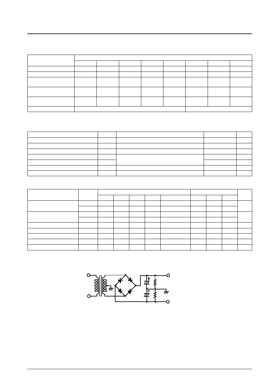
Notes: 1. Unless otherwise noted, use a constant-voltage supply for the power supply used during inspection.
2. Use the transformer power supply circuit stipulated in the figure below for allowable load shorted time measurement and output noise voltage
measurement.
DBA40C
10000
µ
F
10000
µ
F
500
500
+VCC
--VCC
Stipulated Transformer Power Supply (MG-200 equivalent)
3. The output noise voltage values shown are peak values read with a VTVM. However, an AC stabilized (50 Hz) power supply should be used to
minimize the influence of AC primary side flicker noise on the reading.

No. 7065-3/5
STK402-090
Internal Equivalent Circuit
TR4
TR1
TR6
R2
R7
R1
R3
R4
R6
C1
R5
TR3
TR2
1
4
2
13
7
12
5
6
TR5
TR7
TR8
D1
SUB
TR11
TR15
TR13
R14
R9
R13
R11
R12
R8
C2
R10
TR16
TR14
11
9
10
8
14
15
TR12
TR9
TR10
Sample Application Circuit
Ch.1
IN
Ch.1
NF
Pre
-VCC
Pre
+VCC
-VCC
+VCC
BIAS
Ch.2
+VE
Ch.2
NF
SUB
GND
Ch.2
IN
Ch.2
-VE
Ch.1
+VE
Ch.1
-VE
1
2
4
5
6
7
8
9
10
11
12
13
14
15
Ch.2 IN
-VCC
470pF
0.1
µ
F
1.8k
56k
10k
0.22
0.22
0.22
0.22
4.7
33
µ
F
3pF
220pF 2.2
µ
F
1k
56k
100
µ
F
10
µ
F
100
3
µ
H
SUB
Ch.2 OUT
4.7
Ch.1 IN
+VCC
470pF
0.1
µ
F
1.8k
56k
4.7
33
µ
F
3pF
220pF
2.2
µ
F
1k
56k
100
µ
F
10
µ
F
100
3
µ
H
Ch.1 OUT
4.7
Ch.2
Ch.1

No. 7065-4/5
STK402-090
Thermal Design Example
The thermal resistance,
c-a of the required heat sink for the power dissipation, Pd, within the hybrid IC is determined as
follows.
Condition 1: The IC substrate temperature, Tc, must not exceed 125∞C.
Pd
◊
c ≠ a + Ta < 125∞C . . . . . . . . . (1)
Ta: Guaranteed ambient temperature for the end product.
Condition 2: The junction temperature, Tj, of each power transistor must not exceed 150∞C.
Pd
◊
c ≠ a + Pd/N
◊
j ≠ c + Ta < 150∞C . . . . . . . . . (2)
N: Number of power transistors
c-a: Thermal resistance per power transistor
However, the power dissipation, Pd, for the power transistors shall be allocated equally among the N transistors.
The following inequalities results from solving equations (1) and (2) for
c-a.
c ≠ a < (125 ≠ Ta) /Pd . . . . . . . . . . . . . . . . . . (1)'
c ≠ a < (150 ≠ Ta) /Pd ≠
j ≠ c/N . . . . . . . . . (2)'
Values that satisfy these two inequalities at the same time represent the required heat sink thermal resistance.
When the following specifications have been stipulated, the required heat sink thermal resistance can be determined from
formulas (1)' and (2)'.
∑ Supply voltage -- V
CC
∑ Load resistance value -- RL
∑ Guaranteed ambient temperature -- Ta
[Example]
When the IC supply voltage, V
CC
, is ±32 V and R
L
is 6
, the IC internal power dissipation, Pd, will be a maximum of
72 W for a continuous sine wave signal at 1 kHz, according to the Pd ≠ P
O
characteristics.
For the music signals normally handled by audio amplifiers, a value of 1/8 P
O
max is generally used for Pd as an estimate
of the power dissipation based on this type of continuous signal. (Note that the factor used may differ depending on the
safety standards used.)
That is:
Pd = 48 W (When 1/8 P
O
max = 6.25 W)
The number of power transistors in the audio amplifier block of these hybrid ICs, N, is 4, and the thermal resistance per
transistor is 2.2∞C/W. Therefore, the required heat sink thermal resistance for a guaranteed ambient temperature of 50∞C
will be as follows.
From formula (1)'
c ≠ a < (125 ≠ 50) /48
< 1.56
From formula (2)'
c ≠ a < (150 ≠ 50) /48 ≠ 2.2/4
< 1.53
Therefore, 1.53∞C/W is the required heat sink thermal resistance.
Note that this thermal design example assumes the use of a constant-voltage power supply, and is therefore not a verified
design for any particular user's end product.
PS No. 7065-5/5
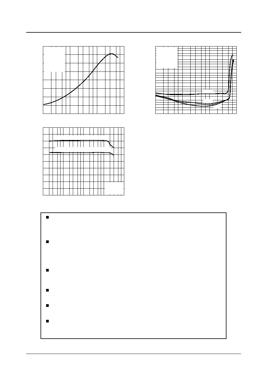
STK402-090
ITF02157
1k
10
100
50
40
30
20
10
0
60
100
80
90
70
2 3
5 7
2 3
5 7
2 3
5 7
2 3
5 7
10k
100k
RL = 6
, VCC =
±
32 V, THD = 10 %
RL = 6
, VCC =
±
32 V, THD = 0.4 %
Tc = 25
∞
C
VG = 30 dB
Rg = 600
PO -- f
Output po
wer
, P
O
-
-
W
Frequency, f - Hz
ITF02155
0.001
1.0
0.1
0.01
7
5
3
2
0.1
7
5
3
2
1.0
7
5
3
2
10
7
5
3
2
100
7
5
3
2
2
3
5
7
2
3
5
7
10
2
3
5
7 100
20 kHz
20 Hz
1 kHz
Tc = 25
∞
C
VCC =
±
32 V
VG = 30 dB
RL = 6
Rg = 600
THD -- PO
T
otal harmonic distortion,
THD
-
- %
Output power, PO -- W
ITF02168
0
1.0
0.1
80
60
70
50
40
30
20
10
2
3
5
7
2
3
5
7
10
2
3
5
7 100
RL = 6
VCC =
±
32 V
f = 1kHz
VG = 30 dB
Rg = 600
2ch drive
Pd -- PO
T
otal de
vice po
wer dissipation Pd
-
-
W
Output power, PO / ch -- W
This catalog provides information as of December, 2002. Specifications and information herein are
subject to change without notice.
Specifications of any and all SANYO products described or contained herein stipulate the performance,
characteristics, and functions of the described products in the independent state, and are not guarantees
of the performance, characteristics, and functions of the described products as mounted in the customer's
products or equipment. To verify symptoms and states that cannot be evaluated in an independent device,
the customer should always evaluate and test devices mounted in the customer's products or equipment.
SANYO Electric Co., Ltd. strives to supply high-quality high-reliability products. However, any and all
semiconductor products fail with some probability. It is possible that these probabilistic failures could
give rise to accidents or events that could endanger human lives, that could give rise to smoke or fire,
or that could cause damage to other property. When designing equipment, adopt safety measures so
that these kinds of accidents or events cannot occur. Such measures include but are not limited to protective
circuits and error prevention circuits for safe design, redundant design, and structural design.
In the event that any or all SANYO products (including technical data, services) described or contained
herein are controlled under any of applicable local export control laws and regulations, such products must
not be exported without obtaining the export license from the authorities concerned in accordance with the
above law.
No part of this publication may be reproduced or transmitted in any form or by any means, electronic or
mechanical, including photocopying and recording, or any information storage or retrieval system,
or otherwise, without the prior written permission of SANYO Electric Co., Ltd.
Any and all information described or contained herein are subject to change without notice due to
product/technology improvement, etc. When designing equipment, refer to the "Delivery Specification"
for the SANYO product that you intend to use.
Information (including circuit diagrams and circuit parameters) herein is for example only; it is not
guaranteed for volume production. SANYO believes information herein is accurate and reliable, but
no guarantees are made or implied regarding its use or any infringements of intellectual property rights
or other rights of third parties.